Node Voltage
Protected power switch, relay driver, and ESD-protected UART module for the PomeLabs Core Kit.
The PomeLabs Node Voltage Module (PML-NV-01) is a multi-function power management and communication protection module — it controls, protects, and isolates in one board. Plug it in and instantly gain a current-limited power switch, a relay driver with built-in flyback protection, and ESD-hardened UART ports, all supervised by your Backend MCU.
Revision: v1.0 | Part Number: PML-NV-01 | Series: PomeLabs Core Kit
Pinout

Schematic

Digital Twin
In the PomeLabs App, the PML-NV-01 module is mirrored as a digital twin in both the Playground and inside any Connect Activity. The twin exposes the power switch, relay driver, and fault monitor as live controls — toggle them on screen and the change is pushed to the physical module over the Connect bus; fault events and rail states are streamed back in real time.
Controls — parameters you can set from the App
Power switch enable · pin GPOUT0 · toggle, HIGH / LOW
Drives the EN pin of U1 (TPS2069EDBVR). HIGH enables the 5V-Protected output rail; LOW disables it and discharges the output through the internal resistor.
Relay control · pin GPOUT1 · toggle, HIGH / LOW
Drives the gate of U2 (SZNUD3124LT1G). HIGH energises relay coil K1; LOW releases it — the internal Zener clamp suppresses inductive kickback automatically.
Monitors — values streamed back from the module
Fault flag · pin GPIN0 · indicator, HIGH / LOW
Reflects the open-drain FLT output of U1 pulled up through R3 ( to 3V3). Goes LOW during overcurrent or overtemperature events; returns HIGH when the fault clears.
5V-Protected rail status · U1 · voltage readout
Confirms the switched output is live and within range. Useful for diagnosing UVLO or soft-start issues.
Relay state · K1 · indicator
Reflects whether the relay coil is energised based on GPOUT1 and U2 gate status.
Datasheet
1. Overview
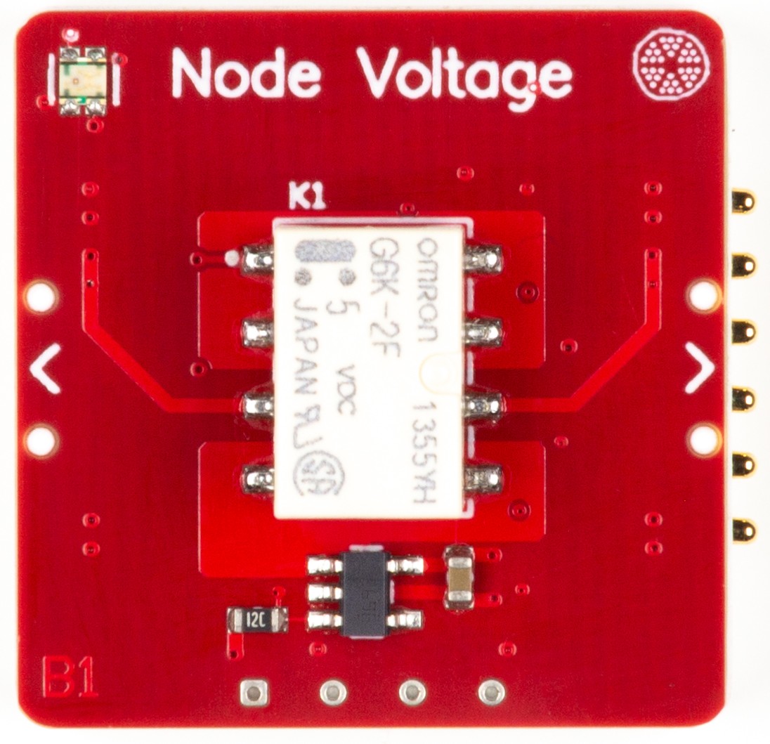
The PML-NV-01 is organised into two functional layers. The FE Function block contains the active power-management circuitry: U1 (TPS2069EDBVR) is a current-limited, software-controlled USB-class power switch that converts a raw 5V-Module input into a protected 5V-Protected output rail under MCU supervision, while U2 (SZNUD3124LT1G) drives a relay coil (K1) directly from a logic-level GPIO with no external free-wheeling diode required. Outside the FE Function block, D1 and D2 (USBLC6-2P6) provide IEC 61000-4-2 Level 4 ESD protection on the two UART communication ports.
This architecture makes the PML-NV-01 the natural bridge between a Backend MCU and any load or node that requires controlled power, galvanic isolation, or hardened communication — without any external protection components.
Key characteristics at a glance:
- U1 (TPS2069EDBVR): active-HIGH continuous-current power switch — built-in soft-start, at , output discharge ( typ), reverse-current blocking, deglitched FLT flag ( typ), and typical short-circuit current limit (±20% accuracy)
- U2 (SZNUD3124LT1G): automotive-grade integrated low-side N-MOSFET relay driver — internal Zener clamp ( typ, max), no external free-wheeling diode required, AEC-Q101 qualified, drives relay coils up to at
- K1 (G6K-2F-DC5): coil DPDT signal relay switched by U2, providing galvanic isolation for the load
- FLT fault reporting from U1 to Backend MCU via GPIN0 (open-drain, pulled up through R3 to 3V3)
- C3 () ceramic input bypass capacitor at U1 IN pin per TI application guidelines
- Compatible with all modules in the PomeLabs Core Kit
2. BOM Components
| Ref. | Type | Value / Part | Role on this module |
|---|---|---|---|
| U1 | Power-distribution switch | TPS2069EDBVR (TI) | Primary power switch. N-channel MOSFET with active-HIGH enable. continuous output, typ short-circuit current limit (±20%). Provides built-in soft-start, output discharge ( = typ), reverse-current blocking, fast typ overcurrent response, and typ deglitched FLT reporting. SOT-23-5 (DBV) package, . |
| U2 | Automotive inductive load driver | SZNUD3124LT1G (onsemi) | Integrated N-channel MOSFET relay driver with internal gate-to-drain and gate-to-source resistors plus internal Zener clamp ( = min, typ) — no external free-wheeling diode required. Logic-level gate input ( = –). Drives relay coil K1 up to continuous. AEC-Q101 qualified. SOT-23 (CASE 318) package. Note: marked as DISCONTINUED by onsemi (not recommended for new designs). |
| D1 | ESD protection IC | USBLC6-2P6 (ST) | IEC 61000-4-2 Level 4 ESD clamp on UART Port 1 (TX_1 / RX_1). Rail-to-rail topology requires VBUS at to clamp positive surges. max I/O-to-GND. SOT-666 (). |
| D2 | ESD protection IC | USBLC6-2P6 (ST) | IEC 61000-4-2 Level 4 ESD clamp on UART Port 2 (TX_2 / RX_2). Identical to D1. |
| K1 | Relay | G6K-2F-DC5 (Omron) | DC coil signal relay switched by U2. Provides galvanic isolation between module logic and switched load. Coil energised when GPOUT1 is driven HIGH by Backend MCU. |
| C3 | MLCC bypass capacitor | Input bypass on 5V-Module rail at U1 IN pin. Required per TI TPS2069E application guidelines ( ceramic close to IN/GND for local noise decoupling). | |
| R1, R2 | Resistor | Pull-up resistors on UART TX/RX lines to 3V3. Hold the lines at a defined HIGH idle state when no node is connected. | |
| R3 | Resistor | Pull-up resistor from FLT pin of U1 to 3V3. Required because FLT is open-drain — without this resistor the fault flag cannot present a HIGH idle level. |
3. Electrical Specifications
All values at unless otherwise noted. Specifications from TI SLVSGZ7C (TPS20xxE, Rev. C, March 2025), onsemi NUD3124/D Rev. 15 (SZNUD3124LT1G, June 2024), and ST DS4260 Rev. 7 (USBLC6-2, December 2021).
3.1 U1 — TPS2069EDBVR
3.1.1 Absolute Maximum Ratings
Exceeding these values may permanently damage the device. Stress ratings only.
| Parameter | Value | Unit |
|---|---|---|
| Input voltage () | to | V |
| Output voltage () | to | V |
| Enable voltage () | to | V |
| FLT pin voltage () | to | V |
| Continuous output current () | Internally limited | — |
| ESD — Human Body Model (HBM) | V | |
| ESD — Charged Device Model (CDM) | V | |
| ESD — IEC 61000-4-2 contact discharge, OUT pin | V | |
| ESD — IEC 61000-4-2 air-gap discharge, OUT pin | V | |
| Junction temperature () | to | °C |
| Storage temperature () | to | °C |
3.1.2 Recommended Operating Conditions
| Parameter | Min | Nom | Max | Unit |
|---|---|---|---|---|
| Input voltage () | V | |||
| Enable input voltage () | — | V | ||
| Enable high-level input voltage () | — | — | V | |
| Enable low-level input voltage () | — | — | V | |
| Continuous output current () | — | — | A | |
| FLT sink current () | — | mA | ||
| Junction temperature () | — | °C | ||
| Ambient operating temperature () | — | °C |
3.1.3 Electrical Characteristics
| Parameter | Min | Typ | Max | Condition |
|---|---|---|---|---|
| at = or | — | — = , over full range | ||
| at = | — | — | — = , = | |
| Output rise time () | — | — = , = , = | ||
| Output fall time () | — | — same conditions as | ||
| Turn-on time () | — | — | — = , = | |
| Turn-off time () | — | — | — same conditions as | |
| Output discharge resistance () | — = = , disabled | |||
| Short-circuit current limit () at | — = , OUT to GND | |||
| Short-circuit current limit () full temp range | — = , OUT to GND | |||
| Overcurrent response time () | — | — | — = , = | |
| Supply current — disabled () at | — | — = | ||
| Supply current — enabled () at | — | — = , = | ||
| UVLO rising threshold | — | — rising | ||
| UVLO hysteresis | — | — | — at | |
| FLT output low voltage () | — | — | — = | |
| FLT off-state leakage | — | — | — = | |
| FLT deglitch time () | — assertion or de-assertion | |||
| Thermal shutdown rising threshold | °C | |||
| Thermal shutdown hysteresis | — | — | °C |
3.2 U2 — SZNUD3124LT1G
3.2.1 Absolute Maximum Ratings
Exceeding these values may permanently damage the device. Stress ratings only.
| Parameter | Value | Unit |
|---|---|---|
| Drain-to-source voltage () — continuous, = | V | |
| Gate-to-source voltage () — continuous, = | V | |
| Drain current () — continuous, = | mA | |
| Single-pulse drain-to-source avalanche energy () | mJ | |
| Peak power dissipation () — square pulse | W | |
| Inductive switching transient () — drain-to-source | V | |
| Reverse battery (), drain-to-source | V | |
| ESD — Human Body Model (HBM) | V | |
| Operating ambient temperature () | to | °C |
| Junction temperature () — max | °C | |
| Storage temperature () | to | °C |
| Total power dissipation — SOT-23, | mW | |
| Thermal resistance junction-to-ambient () — SOT-23 | °C/W |
3.2.2 Electrical Characteristics
| Parameter | Min | Typ | Max | Condition |
|---|---|---|---|---|
| Drain-to-source sustaining voltage () | — = | |||
| Drain-to-source leakage current () | — | — | — = , = , | |
| Gate-body leakage current () | — | — | — = , = , | |
| Gate threshold voltage () | — = , = | |||
| Drain-to-source on-resistance () | — | — | — = , = | |
| Drain-to-source on-resistance () | — | — | — = , = | |
| Output continuous current () | — | — = , = | ||
| High-to-low propagation delay () | — | — | — = , = | |
| Low-to-high propagation delay () | — | — | — same conditions | |
| Rise time () | — | — | — = , = | |
| Fall time () | — | — | — same conditions |
4. Pin Descriptions
All signal pins are referenced to GND.
| Pin / Net Name | Direction | Description |
|---|---|---|
| 5V-Module | Power In | unregulated input supply. Feeds the IN pin of U1. Must be present and stable before EN is asserted. Also drives the K1 relay coil through the U2 low-side switch. |
| 5V-Protected | Power Out | Switched, current-limited output from U1 OUT pin. Active only when GPOUT0 is HIGH. Protected against short circuits and overcurrent ( typ limit, continuous rating). When U1 is disabled, the output is actively discharged through . |
| 3V3 | Power In | logic rail. Supplies the VBUS pin of D1/D2 (required for ESD clamp topology), the FLT pull-up R3, and the UART pull-ups R1/R2. |
| GPOUT0 | Input | GPIO from Backend MCU. Drives the EN pin of U1. Pull HIGH () to enable 5V-Protected; pull LOW () to disable. Must not be left floating. |
| GPOUT1 | Input | GPIO from Backend MCU. Drives the Gate of U2 through the internal resistor. Drive HIGH ( worst-case to fully turn on) to energise relay coil K1; drive LOW to release the relay. |
| GPIN0 | Output (to MCU) | Open-drain FLT signal from U1, pulled up to 3V3 through R3 (). Active-LOW; asserted during overcurrent or thermal shutdown. The fault is deglitched by typ on both edges. |
| TX_1-L / TX_2-L | Input | UART transmit from Backend MCU (USART1/USART2). Routed through D1/D2 ESD protection to the node-side connectors. |
| RX_1-L / RX_2-L | Output | UART receive from node connectors back to Backend MCU. Passed through D1/D2 ESD protection. |
| GND | Ground | Common ground reference shared across all ICs, the relay coil return path, and all connectors. |
5. Connection Guide & Common Errors
Correct power-up sequence:
- Connect GND first, ensuring it is shared across the Backend MCU, the PML-NV-01, and any downstream load on the common bus.
- Connect 5V-Module to a regulated source. U1 remains in shutdown (output disabled, output actively discharged through ) until GPOUT0 is asserted HIGH.
- Connect the 3V3 rail. This provides bias for the FLT pull-up R3, the UART pull-ups R1/R2, and the VBUS pin of the ESD ICs D1/D2.
- After both supplies are stable, drive GPOUT0 HIGH to enable 5V-Protected. Soft-start ramps the output in typ ( max at = into / ).
- Drive GPOUT1 HIGH only after the load side is ready. The relay K1 energises in roughly – (typ propagation delay through U2 ; the rest is mechanical).
- Read GPIN0 in firmware to detect FLT events. The signal is debounced internally — a transient overload shorter than (typ) does not assert FLT, and a fault must persist (typ) before GPIN0 goes LOW.
Note on FLT timing: the (–) deglitch window means software cannot rely on FLT to detect very short overcurrent events. Conversely, when clearing a fault by toggling EN, allow the deglitch period to elapse before re-arming the load.
Common wiring errors and consequences:
| Mistake | Symptom | Correction |
|---|---|---|
| EN pin (GPOUT0) left floating | Output state is undefined per TI; charge-pump bias is unstable; 5V-Protected may glitch on or off | Always drive EN actively from GPOUT0. Tie to GND if the rail must be permanently OFF. EN must not be left open per the TI datasheet. |
| FLT pull-up R3 missing or rail floating | FLT line never goes HIGH (it is open-drain) — Backend MCU sees a permanent or floating fault and cannot distinguish good from faulted state | Connect R3 = from FLT to 3V3. 3V3 rail must be live for the pull-up to do its job. |
| Input bypass C3 too small or absent | Local noise/inrush at turn-on causes to dip below the UVLO threshold () — U1 may UVLO-cycle on power-up; long input cables can also drive above the absolute max via inductive overshoot | Place a ceramic capacitor close to IN/GND per TI guideline. For long input cables or noisy supplies, add a – ceramic (or a on OUT) to absorb transients. |
| 5V-Module exceeds (or abs max) | U1 permanently damaged | Keep 5V-Module within the – recommended operating range. Never exceed absolute max. |
| GPOUT1 high level too low for U2 gate | U2 MOSFET does not fully enhance — high , relay may not pull in cleanly, MOSFET dissipates excessive power | is min / max. Drive GPOUT1 to guarantee full enhancement; is ideal. The internal + network leaves the MOSFET OFF when GPOUT1 floats. |
| Free-wheeling diode added across K1 coil externally | Inductive kickback bypasses the U2 internal Zener clamp, slowing relay drop-out and partially defeating the integrated solution | U2's internal Zener clamp ( = min, typ) absorbs the kickback by design — no external free-wheeling diode is required or recommended. |
| Relay coil current exceeds | U2 rating exceeded; thermal stress on the SOT-23 ( max dissipation) | Verify the K1 coil current at the operating supply voltage. The G6K-2F-DC5 has a coil resistance well above , keeping well within spec. |
| 5V-Module and 5V-Protected shorted together externally | Bypasses U1's short-circuit protection — the upstream supply sees the load directly with no current limit | Keep 5V-Module and 5V-Protected as separate nets. Only U1 bridges them. |
| USBLC6-2P6 VBUS pin unconnected on D1 or D2 | Rail-to-rail ESD topology cannot clamp positive surges — UART RX pins exposed to direct ESD | Connect VBUS of both D1 and D2 to the 3V3 rail (or to 5V-Protected per the schematic). The rail must be powered before any cable is mated to a UART port. |
| Reading FLT immediately after enabling U1 | False fault reported during the soft-start window | FLT is high-impedance during UVLO, and the deglitch may not have settled. Wait at least after asserting EN before sampling GPIN0. |
| Designing a new product around U2 | SZNUD3124LT1G is marked "DISCONTINUED — not recommended for new design" by onsemi (NUD3124/D Rev. 15) | For new designs, contact onsemi for a recommended replacement (e.g. NCV8402 series or a discrete logic-level MOSFET + flyback diode). The PML-NV-01 retains the part for legacy compatibility only. |
Hands-on Labs
Get started with the PML-NV-01 through guided labs that combine onboarding with progressive practice exercises. Each lab opens in the PomeLabs app.
Node Voltage Onboarding
Power up the module, verify the 5V-Protected rail, and trigger your first fault event. Recommended starting point.
Current-Limited Power Switch
Control the TPS2069E power switch via GPIO, intentionally trigger an overcurrent fault, and observe the FLT flag response.
Relay Driver
Energise and de-energise relay K1 from a logic-level GPIO, observe inductive kickback suppression by the internal Zener clamp, and measure switching delays.
ESD-Protected UART
Send and receive data through the USBLC6-2P6 protected ports and verify signal integrity under ESD stress conditions.
Use Cases
Coming soon.
How is this guide?